Central Processing Unit
The central processing unit (CPU) is the portion of a computer system that carries out the instructions of a computer program, to perform the basic arithmetical, logical, and input/output operations of the system. The CPU plays a role somewhat analogous to the brain in the computer. The term has been in use in the computer industry at least since the early 1960s. The form, design and implementation of CPUs have changed dramatically since the earliest examples, but their fundamental operation remains much the same.
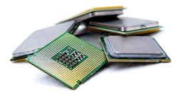
On large machines, CPUs require one or more printed circuit boards. On personal computers and small workstations, the CPU is housed in a single silicon chip called a microprocessor. Since the 1970s the microprocessor class of CPUs has almost completely overtaken all other CPU implementations. Modern CPUs are large scale integrated circuits in packages typically less than four centimeters square, with hundreds of connecting pins.
Two typical components of a CPU are the arithmetic logic unit (ALU), which performs arithmetic and logical operations, and the control unit (CU), which extracts instructions from memory and decodes and executes them, calling on the ALU when necessary.
Not all computational systems rely on a central processing unit. An array processor or vector processor has multiple parallel computing elements, with no one unit considered the "center". In the distributed computing model, problems are solved by a distributed interconnected set of processors.
Computers such as the ENIAC had to be physically rewired to perform different tasks, which caused these machines to be called "fixed-program computers." Since the term "CPU" is generally defined as a device for software (computer program) execution, the earliest devices that could rightly be called CPUs came with the advent of the stored-program computer.
The idea of a stored-program computer was already present in the design of J. Presper Eckert and John William Mauchly's ENIAC, but was initially omitted so that it could be finished sooner. On June 30, 1945, before ENIAC was made, mathematician John von Neumann distributed the paper entitled First Draft of a Report on the EDVAC. It was the outline of a stored-program computer that would eventually be completed in August 1949. EDVAC was designed to perform a certain number of instructions (or operations) of various types. These instructions could be combined to create useful programs for the EDVAC to run. Significantly, the programs written for EDVAC were stored in high-speed computer memory rather than specified by the physical wiring of the computer. This overcame a severe limitation of ENIAC, which was the considerable time and effort required to reconfigure the computer to perform a new task. With von Neumann's design, the program, or software, that EDVAC ran could be changed simply by changing the contents of the memory.
Early CPUs were custom-designed as a part of a larger, sometimes one-of-a-kind, computer. However, this method of designing custom CPUs for a particular application has largely given way to the development of mass-produced processors that are made for many purposes. This standardization began in the era of discrete transistor mainframes and minicomputers and has rapidly accelerated with the popularization of the integrated circuit (IC). The IC has allowed increasingly complex CPUs to be designed and manufactured to tolerances on the order of nanometers. Both the miniaturization and standardization of CPUs have increased the presence of digital devices in modern life far beyond the limited application of dedicated computing machines. Modern microprocessors appear in everything from automobiles to cell phones and children's toys.
While von Neumann is most often credited with the design of the stored-program computer because of his design of EDVAC, others before him, such as Konrad Zuse, had suggested and implemented similar ideas. The so-called Harvard architecture of the Harvard Mark I, which was completed before EDVAC, also utilized a stored-program design using punched paper tape rather than electronic memory. The key difference between the von Neumann and Harvard architectures is that the latter separates the storage and treatment of CPU instructions and data, while the former uses the same memory space for both. Most modern CPUs are primarily von Neumann in design, but elements of the Harvard architecture are commonly seen as well.
Relays and vacuum tubes (thermionic valves) were commonly used as switching elements; a useful computer requires thousands or tens of thousands of switching devices. The overall speed of a system is dependent on the speed of the switches. Tube computers like EDVAC tended to average eight hours between failures, whereas relay computers like the (slower, but earlier) Harvard Mark I failed very rarely. In the end, tube based CPUs became dominant because the significant speed advantages afforded generally outweighed the reliability problems. Most of these early synchronous CPUs ran at low clock rates compared to modern microelectronic designs (see below for a discussion of clock rate). Clock signal frequencies ranging from 100 kHz to 4 MHz were very common at this time, limited largely by the speed of the switching devices they were built with.
Microprocessors
In the 1970s the fundamental inventions by Federico Faggin (Silicon Gate MOS ICs with self aligned gates along with his new random logic design methodology) changed the design and implementation of CPUs forever. Since the introduction of the first commercially available microprocessor (the Intel 4004) in 1970, and the first widely used microprocessor (the Intel 8080) in 1974, this class of CPUs has almost completely overtaken all other central processing unit implementation methods. Mainframe and minicomputer manufacturers of the time launched proprietary IC development programs to upgrade their older computer architectures, and eventually produced instruction set compatible microprocessors that were backward-compatible with their older hardware and software. Combined with the advent and eventual vast success of the now ubiquitous personal computer, the term CPU is now applied almost exclusively to microprocessors. Several CPUs can be combined in a single processing chip.
Previous generations of CPUs were implemented as discrete components and numerous small integrated circuits (ICs) on one or more circuit boards. Microprocessors, on the other hand, are CPUs manufactured on a very small number of ICs; usually just one. The overall smaller CPU size as a result of being implemented on a single die means faster switching time because of physical factors like decreased gate parasitic capacitance. This has allowed synchronous microprocessors to have clock rates ranging from tens of megahertz to several gigahertz. Additionally, as the ability to construct exceedingly small transistors on an IC has increased, the complexity and number of transistors in a single CPU has increased dramatically. This widely observed trend is described by Moore's law, which has proven to be a fairly accurate predictor of the growth of CPU (and other IC) complexity to date.
While the complexity, size, construction, and general form of CPUs have changed drastically over the past sixty years, it is notable that the basic design and function has not changed much at all. Almost all common CPUs today can be very accurately described as von Neumann stored-program machines. As the aforementioned Moore's law continues to hold true, concerns have arisen about the limits of integrated circuit transistor technology. Extreme miniaturization of electronic gates is causing the effects of phenomena like electromigration and subthreshold leakage to become much more significant. These newer concerns are among the many factors causing researchers to investigate new methods of computing such as the quantum computer, as well as to expand the usage of parallelism and other methods that extend the usefulness of the classical von Neumann model.
Operation
The fundamental operation of most CPUs, regardless of the physical form they take, is to execute a sequence of stored instructions called a program. The program is represented by a series of numbers that are kept in some kind of computer memory. There are four steps that nearly all CPUs use in their operation: fetch, decode, execute, and writeback.
The first step, fetch, involves retrieving an instruction (which is represented by a number or sequence of numbers) from program memory. The location in program memory is determined by a program counter (PC), which stores a number that identifies the current position in the program. After an instruction is fetched, the PC is incremented by the length of the instruction word in terms of memory units. Often, the instruction to be fetched must be retrieved from relatively slow memory, causing the CPU to stall while waiting for the instruction to be returned. This issue is largely addressed in modern processors by caches and pipeline architectures (see below).
The instruction that the CPU fetches from memory is used to determine what the CPU is to do. In the decode step, the instruction is broken up into parts that have significance to other portions of the CPU. The way in which the numerical instruction value is interpreted is defined by the CPU's instruction set architecture (ISA). Often, one group of numbers in the instruction, called the opcode, indicates which operation to perform. The remaining parts of the number usually provide information required for that instruction, such as operands for an addition operation. Such operands may be given as a constant value (called an immediate value), or as a place to locate a value: a register or a memory address, as determined by some addressing mode. In older designs the portions of the CPU responsible for instruction decoding were unchangeable hardware devices. However, in more abstract and complicated CPUs and ISAs, a microprogram is often used to assist in translating instructions into various configuration signals for the CPU. This microprogram is sometimes rewritable so that it can be modified to change the way the CPU decodes instructions even after it has been manufactured.
After the fetch and decode steps, the execute step is performed. During this step, various portions of the CPU are connected so they can perform the desired operation. If, for instance, an addition operation was requested, the arithmetic logic unit (ALU) will be connected to a set of inputs and a set of outputs. The inputs provide the numbers to be added, and the outputs will contain the final sum. The ALU contains the circuitry to perform simple arithmetic and logical operations on the inputs (like addition and bit wise operations). If the addition operation produces a result too large for the CPU to handle, an arithmetic overflow flag in a flags register may also be set.
The final step, writeback, simply "writes back" the results of the execute step to some form of memory. Very often the results are written to some internal CPU register for quick access by subsequent instructions. In other cases results may be written to slower, but cheaper and larger, main memory. Some types of instructions manipulate the program counter rather than directly produce result data. These are generally called "jumps" and facilitate behavior like loops, conditional program execution (through the use of a conditional jump), and functions in programs. Many instructions will also change the state of digits in a "flags" register. These flags can be used to influence how a program behaves, since they often indicate the outcome of various operations. For example, one type of "compare" instruction considers two values and sets a number in the flags register according to which one is greater. This flag could then be used by a later jump instruction to determine program flow.
After the execution of the instruction and writeback of the resulting data, the entire process repeats, with the next instruction cycle normally fetching the next-in-sequence instruction because of the incremented value in the program counter. If the completed instruction was a jump, the program counter will be modified to contain the address of the instruction that was jumped to, and program execution continues normally. In more complex CPUs than the one described here, multiple instructions can be fetched, decoded, and executed simultaneously. This section describes what is generally referred to as the "classic RISC pipeline", which in fact is quite common among the simple CPUs used in many electronic devices (often called microcontroller). It largely ignores the important role of CPU cache, and therefore the access stage of the pipeline.
Design and implementation
The basic concept of a CPU is as follows:
Hardwired into a CPU's design is a list of basic operations it can perform, called an instruction set. Such operations may include adding or subtracting two numbers, comparing numbers, or jumping to a different part of a program. Each of these basic operations is represented by a particular sequence of bits; this sequence is called the opcode for that particular operation. Sending a particular opcode to a CPU will cause it to perform the operation represented by that opcode. To execute an instruction in a computer program, the CPU uses the opcode for that instruction as well as its arguments (for instance the two numbers to be added, in the case of an addition operation). A computer program is therefore a sequence of instructions, with each instruction including an opcode and that operation's arguments.
The actual mathematical operation for each instruction is performed by a subunit of the CPU known as the arithmetic logic unit or ALU. In addition to using its ALU to perform operations, a CPU is also responsible for reading the next instruction from memory, reading data specified in arguments from memory, and writing results to memory.
In many CPU designs, an instruction set will clearly differentiate between operations that load data from memory, and those that perform math. In this case the data loaded from memory is stored in registers, and a mathematical operation takes no arguments but simply performs the math on the data in the registers and writes it to a new register, whose value a separate operation may then write to memory.
Integer range
The way a CPU represents numbers is a design choice that affects the most basic ways in which the device functions. Some early digital computers used an electrical model of the common decimal (base ten) numeral system to represent numbers internally. A few other computers have used more exotic numeral systems like ternary (base three). Nearly all modern CPUs represent numbers in binary form, with each digit being represented by some two-valued physical quantity such as a "high" or "low" voltage.
MOS 6502 microprocessor in a dual in-line package, an extremely popular 8-bit designRelated to number representation is the size and precision of numbers that a CPU can represent. In the case of a binary CPU, a bit refers to one significant place in the numbers a CPU deals with. The number of bits (or numeral places) a CPU uses to represent numbers is often called "word size", "bit width", "data path width", or "integer precision" when dealing with strictly integer numbers (as opposed to floating point). This number differs between architectures, and often within different parts of the very same CPU. For example, an 8-bit CPU deals with a range of numbers that can be represented by eight binary digits (each digit having two possible values), that is, 28 or 256 discrete numbers. In effect, integer size sets a hardware limit on the range of integers the software run by the CPU can utilize.
Integer range can also affect the number of locations in memory the CPU can address (locate). For example, if a binary CPU uses 32 bits to represent a memory address, and each memory address represents one octet (8 bits), the maximum quantity of memory that CPU can address is 232 octets, or 4 GiB. This is a very simple view of CPU address space, and many designs use more complex addressing methods like paging to locate more memory than their integer range would allow with a flat address space.
Higher levels of integer range require more structures to deal with the additional digits, and therefore more complexity, size, power usage, and general expense. It is not at all uncommon, therefore, to see 4- or 8-bit microcontrollers used in modern applications, even though CPUs with much higher range (such as 16, 32, 64, even 128-bit) are available. The simpler microcontrollers are usually cheaper, use less power, and therefore generate less heat, all of which can be major design considerations for electronic devices. However, in higher-end applications, the benefits afforded by the extra range (most often the additional address space) are more significant and often affect design choices. To gain some of the advantages afforded by both lower and higher bit lengths, many CPUs are designed with different bit widths for different portions of the device. For example, the IBM System/370 used a CPU that was primarily 32 bit, but it used 128-bit precision inside its floating point units to facilitate greater accuracy and range in floating point numbers. Many later CPU designs use similar mixed bit width, especially when the processor is meant for general-purpose usage where a reasonable balance of integer and floating point capability is required.
Performance
The performance or speed of a processor depends on the clock rate (generally given in multiples of hertz) and the instructions per clock (IPC), which together are the factors for the instructions per second (IPS) that the CPU can perform. Many reported IPS values have represented "peak" execution rates on artificial instruction sequences with few branches, whereas realistic workloads consist of a mix of instructions and applications, some of which take longer to execute than others. The performance of the memory hierarchy also greatly affects processor performance, an issue barely considered in MIPS calculations. Because of these problems, various standardized tests, often called "benchmarks" for this purpose—such as SPECint -- have been developed to attempt to measure the real effective performance in commonly used applications.
Processing performance of computers is increased by using multi-core processors, which essentially is plugging two or more individual processors (called cores in this sense) into one integrated circuit. Ideally, a dual core processor would be nearly twice as powerful as a single core processor. In practice, however, the performance gain is far less, only about 50%, due to imperfect software algorithms and implementation. Increasing the number of cores in a processor (i.e. dual-core, quad-core, etc.) increases the workload that a computer can handle. This means that the processor can now handle numerous asynchronous events, Interrupts, etc. which can take a toll on the CPU (Central Processing Unit) when overwhelmed. It is best to think of these numerous cores as different floors in a processing plant, with each floor handling a different task. Sometimes, these cores will handle the same tasks as cores adjacent to them if a single core is not enough to handle the information to prevent a crash.
Processing performance of computers is increased by using multi-core processors, which essentially is plugging two or more individual processors (called cores in this sense) into one integrated circuit. Ideally, a dual core processor would be nearly twice as powerful as a single core processor. In practice, however, the performance gain is far less, only about 50%, due to imperfect software algorithms and implementation. Increasing the number of cores in a processor (i.e. dual-core, quad-core, etc.) increases the workload that a computer can handle. This means that the processor can now handle numerous asynchronous events, Interrupts, etc. which can take a toll on the CPU (Central Processing Unit) when overwhelmed. It is best to think of these numerous cores as different floors in a processing plant, with each floor handling a different task. Sometimes, these cores will handle the same tasks as cores adjacent to them if a single core is not enough to handle the information to prevent a crash.
